Design and Implement of QPSK Modem Based on FPGA.
Abstract :
This paper presents a
method to designs QPSK modulator and demodulator of a spread spectrum system
which use field programmable device. The method uses the tool of
Quartus Ⅱ of American Altera Co. The whole system is divided into several small
models based on top-down design method, and using VHDL hardware description
language to design each model.
The direct digital synthesis (DDS) principle is
briefly presented and used to design orthogonal cosine signal module. In
demodulator, we use the low pass FIR filtering to filter high frequency
component. The QPSK module is ultimately implemented on the FPGA device.
The
whole system has been simulated in the Quartus II7.2 simulation environment
and successfully downloaded to the chip of the Cyclone II EP2C5F256C6. The
operating results and the theoretical results are consistent, so it’s verified
the correctness of this design. The results showed that the
proposed method can greatly improve the developing efficiency, shorten
developing period and reduce costs.
INTRODUCTION:
An SDR(Software
Defined Radio) is a radio in which the properties of carrier
frequency, signal bandwidth, modulation, and network access are defined by
software. Today’s SDR, in contrast, is a general-purpose device in which the
same radio tuner and processors are used to implement many waveforms at many
frequencies. It’s idea is to get the software as close to the antenna as is
feasible. Ultimately, we're turning hardware problems into software problems.
The advantage of this approach is that the equipment is more versatile and
cost-effective. This paper design and implement QPSK modulator and demodulator based
on SDR ideology. QPSK modulation ordinarily use modem chips, or ASIC to
implement, but those chips usually don’t have sufficient Programming skills and
its functionality can not easily be changed or improved in the product
development process. Therefore, those chips are not suitable the situation
where the parameters changed frequently.
The communication system based on FPGA
is easy to implement the pipeline architecture and simple to upgrade. This is a
very practical approach to implement the QPSK modulator and demodulator. DDS is
a new technology of Frequency Synthesis.
It develops the third generation of Frequency
Synthesis Technology after Direct Frequency Synthesis and Indirect Frequency
Synthesis, and breaks through the theory of the former two methods of Frequency
Synthesis. Reference [1] pointed that the technique of DDS is gaining
popularity as a method of generating sinusoidal signals and modulated signals
in digital systems.
BLOCK DIAGRAM:
 Design and Implement of QPSK Modem Based on FPGA. |
A. The Model of DDS:
In the simplest case a Direct Digital Synthesis is constructed
by a ROM with many samples of a sine wave stored in it (sine look-up table,
LUT) and it was introduced in [2]-[3]. Figure.1 shows the block diagram of a
DDS system. The DDS produces sinusoidal signals at a given frequency by digital
integration of a higher clock frequency. The Phase Accumulator stage accepts
the so called Frequency Setting Word (FSW) which determines the phase step.
Once set, this digital word determines the sine wave frequency to be produced.
The phase accumulator then continuously produces in the output proper binary
words indicating the instantaneous phase to the table look-up function. In other
words the phase accumulator is used to "calculate" the successive
addresses of the sine look-up table which generates a digital sine-wave output.
In this way the samples are swept in a controlled manner i.e. with a step depending
on the Frequency Setting Word. The DDS translates the resulting phase to a
sinusoidal waveform via the look-up table, and converts the digital
representation of the sine-wave to analog form using a Digital-to-Analog Converter
followed by a low pass filter (LPF).
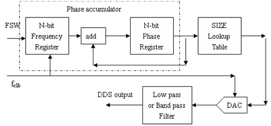
Figure 1. Block Diagram of a DDS System
B. The model of QPSK:
A
QPSK signal is generated by two BPSK signal and it was introduced in [4]. To
distinguish the two signals, we use two orthogonal carrier signals. One is
given by cos(2 ) c πf t , and the other is given by sin(2 ) c πf t .
The two carrier signals remain orthogonal in the area of a period. By using
cos(2 ) c πf t and sin(2 ) c
πf t , we can represent QPSK signals by: ( ) 1 ( ) cos(2
) 1 ( )sin(2 ) (2) 2 2 I c Q c s t =
d t πf t + d t πf t At the receiver, the received signal is down converted
to the baseband by multiplying it by the carrier frequency. Then in both I and
Q channels, the down-converted signal is filtered by FIR filter. The signals
are then adjudged, and the transmitted digital is recovered. QPSK basically
uses the configuration shown in Figure.2 with several blocks, specialized for
QPSK.
REFERENCES:
[1] M.
L. Welborn, “Direct Waveform Synthesis for Software Radios,”
IEEE
Wireless Communications and Networking Conference WCNC. 1999, vol. 1, pp.
211-215, September 1999.
[2] C.
S. Koukourlis, J. E .Plevridis, J. N. Sahalos, “A New Digital Implementation of
the RDS in the FM Stereo,” IEEE Trans. Broadcast, vol. 42, pp. 323-327,
December 1996.
[3]
Wenmiao Song, Jingying Zhang, Qiongqiong Yao, “Design And Implement Of BPSK
Modulator And Demodulator Based On Moder DSP Technology,” IEEE International
Symposium. pp. 1135-1137, 2009.
[4]
Hiroshi Harada, Ramjee Prasad, “Simulation and Software Radio for Mobile Communications,”
Artech House Publishers Bk&CD-Rom edition. pp. 90-93,2002.